← Today's ranking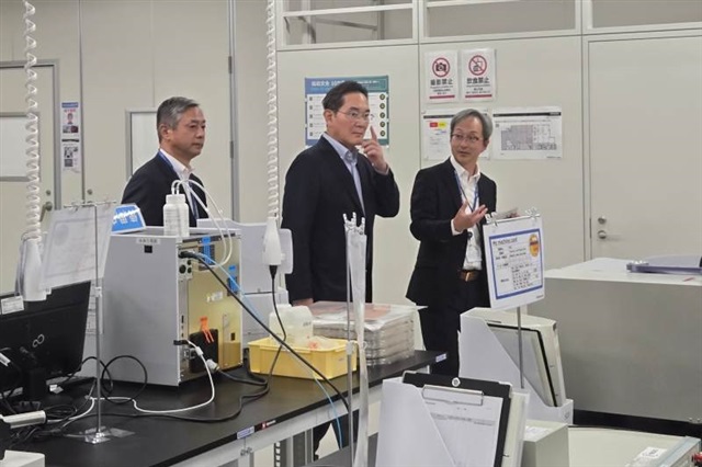
Samsung chairman Lee Jae-yong turns to Japan for AI chip packaging edge
Samsung chairman visits Japan lab to strengthen advanced semiconductor packaging capabilities.
“Samsung Electronics chairman Lee Jae-yong visited the company's Advanced Package Lab (APL) in Yokohama, Japan, on November 1, as the chipmaker looks to Japan's semiconductor…”
Why it matters
Samsung's turn to Japan for advanced packaging capabilities exposes a gap in its in-house expertise and signals where US fabs may also need partnerships. Packaging becomes a critical bottleneck for AI chip competitiveness, affecting which suppliers consolidate and gain pricing power.
AI score breakdown
#21 that day3.00/ 10
A composite of 3.00/10 put this story at #21 for Tuesday, November 3, 2026, driven mostly by technology breakthrough (4/10) and economic impact (4/10).
Technology breakthrough · weight 30%4/10
Economic impact · weight 25%4/10
Job impact · weight 20%2/10
Regional relevance · weight 15%2/10
Policy & geopolitics · weight 10%1/10
Composite is the weighted sum of the five dimensions. How scoring works →
Companies in this story
Related stories
- Intel 18A yields hit 70% as company signs Microsoft as EMIB customer · 2026-11-20
- Intel signs first external customer for advanced 18A chips · 2026-11-19
- Governor Hochul Celebrates the Groundbreaking of GlobalFoundries’ New $10 Billion Semiconductor Manufacturing Facility in Saratoga County · 2026-11-16
- GlobalFoundries breaks ground on first new semiconductor fab under landmark U.S.-Japan initiative · 2026-11-14
- [News] Decoding Impact: Asia Chipmakers Move to Tackle Helium Strain as Intel Gains Relative Buffer · 2026-04-09