Samsung makes world’s first 900-layer storage chip
Samsung demonstrates world's first 900-layer V-NAND prototype amid AI demand surge.
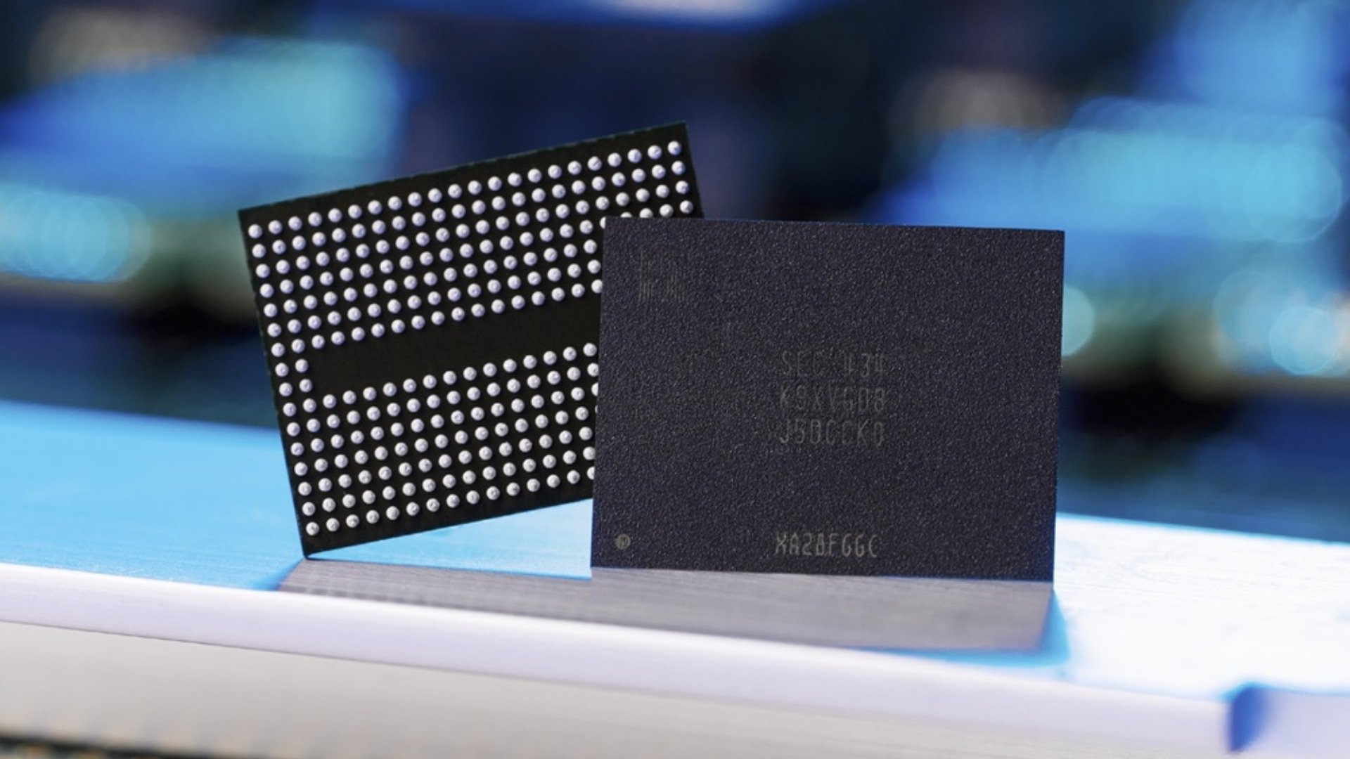
“Samsung, the world’s largest memory chip maker, has reportedly created the world’s first 900-layer V-NAND flash storage chip prototype. At a time when AI growth…”
Why it matters
Weekly Silicon's editorial model scored this 4.50/10 overall, reading it above all as a chipmaking story — news about how and where silicon actually gets made. Its strongest dimension is technology breakthrough at 7/10 — a genuine capability or engineering advance rather than a routine product update — with economic impact close behind at 6/10, pointing to meaningful consequences for capital, capacity, or competition across the industry. The impact is global rather than tied to one US hub, so the thing to watch is how it filters into domestic supply chains and hiring.
Derived from the AI score breakdown below.
AI score breakdown
A composite of 4.50/10 put this story at #6 for Tuesday, May 26, 2026, driven mostly by technology breakthrough (7/10) and economic impact (6/10).
Composite is the weighted sum of the five dimensions. How scoring works →
Companies in this story
Related stories
- How agentic AI and 'AI physics' are reshaping chip design · 2026-09-05
- Silicon Labs Opens New Austin Innovation Center with Support from Texas CHIPS Act · 2026-09-05
- GlobalWafers outlines US expansion plans at SEMICON Taiwan, eyes $7.5B total investment · 2026-09-02
- Tesla advances Austin chip facility as Musk's Texas Terafab takes shape - Austin American-Statesman · 2026-09-01
- SK Hynix to start AI chip output in Indiana in 2029, sees memory shortage through 2030 · 2026-08-30