TSMC says panel packaging won't replace CoWoS anytime soon for the largest future AI processors — wafer-level tech can scale to 58 massive dies in one package
TSMC confirms wafer-level CoWoS remains superior to panel packaging for large AI chips.
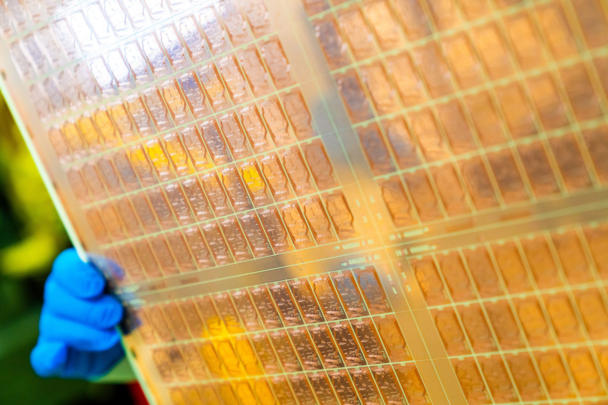
“TSMC is exploring panel-level packaging and is working on its CoPoS technology, but the company's Kevin Zhang says wafer-level packaging technologies is considerably more advanced…”
Why it matters
Weekly Silicon's editorial model scored this 3.80/10 overall, reading it above all as an industry story with cross-cutting implications. Its strongest dimension is technology breakthrough at 5/10 — a genuine capability or engineering advance rather than a routine product update — with economic impact close behind at 5/10, pointing to meaningful consequences for capital, capacity, or competition across the industry. The impact is global rather than tied to one US hub, so the thing to watch is how it filters into domestic supply chains and hiring.
Derived from the AI score breakdown below.
AI score breakdown
A composite of 3.80/10 put this story at #3 for Wednesday, June 17, 2026, driven mostly by technology breakthrough (5/10) and economic impact (5/10).
Composite is the weighted sum of the five dimensions. How scoring works →
Companies in this story
Related stories
- AMD invests over $10B in Taiwan for advanced chip packaging with TSMC · 2026-08-24
- TSMC Completes 1.6nm A16 Chip Process, Widening Technology Gap With Rival Samsung Electronics Ahead of Q4 · 2026-08-24
- TSMC readies 1.6nm A16 chips for Q4 mass production, targets AI and HPC - CHOSUNBIZ · 2026-08-20
- Microsoft's Maia 300 Chip Targets NVIDIA's AI Dominance · 2026-08-17
- Inside Intel: how America’s chip champion came back from the brink · 2026-08-14